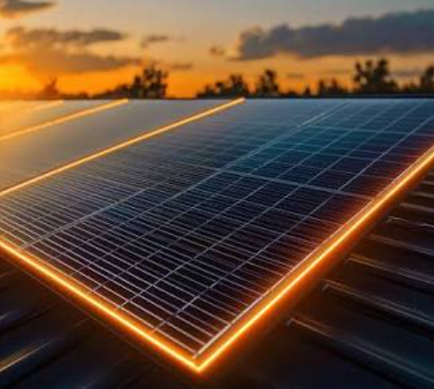
Maintaining long-term efficiency and structural integrity in photovoltaic (PV) systems requires robust semiconductor engineering across both power conversion stages and module-level protection schemes. From high-efficiencyphotovoltaic power conversion topologies inside grid-tied inverters down to the specialized bypass diodes mounted inside panel junction boxes, selecting reliable components directly dictates systemic levelized cost of energy (LCOE) and operational safety.
1. Solar Inverter Power Architecture
A grid-tied PV inverter converts fluctuating DC array voltage into clean, grid-synchronized AC power using a multi-stage topology:
┌─────────────────┐ ┌──────────────────────────┐ ┌──────────────────────────┐
│ PV Array Input │ ───► │ DC-DC Boost Stage (MPPT) │ ───► │ DC-AC Inversion Stage │ ───► Utility Grid
│ (Variable DC) │ │ Fast MOSFETs / SiC Diodes│ │ IGBTs / Neutral-Point │ (50/60 Hz AC)
└─────────────────┘ └──────────────────────────┘ └──────────────────────────┘
DC-DC Boost & MPPT Stage
- Function: Maximizes energy extraction across varying solar irradiance levels by continuously adjusting input impedance.
- Component Requirements: High-voltage Superjunction MOSFETs or Shielded Gate Trench (SGT) MOSFETs operating at elevated switching frequencies (50kHz to 100kHz) allow smaller passive inductors. Pairing active switches with ultra-fast recovery or SiC Schottky diodes minimizes reverse recovery energy losses (Erec).
DC-AC Inversion Stage
- Function: Converts high-voltage DC bus potential into AC current.
- Component Requirements: Inverters utilization 3-Level Neutral-Point Clamped (NPC) or T-type topologies rely on Field-Stop Trench IGBTs. IGBTs combine low collector-emitter saturation voltages (VCE(sat)) with continuous high-current density to keep thermal dissipation manageable under heavy loads.
2. Array Protection: The Role of Bypass Diodes
While inverters handle active power conversion, individual PV modules face physical threats from environmental factors like partial shading (e.g., from trees, dirt, or clouds).
Unprotected Shaded Sub-String
┌──────┐ ┌──────┐ ┌──────────────┐ ┌──────┐
│ Cell │───►│ Cell │───►│ Shaded Cell │───►│ Cell │ ===> High Reverse Bias + Extreme Heating
└──────┘ └──────┘ │ (High Resistance) └──────┘ (Risk of Hot-Spot Thermal Runaway)
└──────────────┘
│
Bypass Diode Added
▼
┌──────┐ ┌──────┐ ┌──────────────┐ ┌──────┐
│ Cell │───►│ Cell │────┤ Shaded Cell ├────│ Cell │
└──────┘ └──────┘ └──────┬───────┘ └──────┘
│ │ Forward │
└───┴─◄───[▶|]──┴─── Output Current Bypasses
Diode Shaded Cell Section
The Hot-Spot Mechanism
When a solar cell within a series-connected string is shaded, it ceases to generate current and transitions into a high-resistance load. Illuminated cells in the string force string current through the shaded cell, driving it into reverse bias. The resulting power dissipation (P=IVreverse) concentrates severe heat into a small surface area, creating a hot spot capable of melting encapsulants, cracking front glass, or igniting fires.
Bypass Protection Mechanics
Bypass diodes are connected in anti-parallel across small sub-strings of solar cells (typically 18–24 cells per diode) inside the module junction box.
- Normal Illumination: The diode is reverse-biased by the panel’s generated voltage and remains in an OFF state.
- Partial Shading: As the shaded cell enters reverse bias, the potential across the sub-string flips, forward-biasing the bypass diode. Current routes through the low-impedance diode path, isolating the shaded section while allowing the remaining unshaded sub-strings to continue producing power.
See also: The Integral Role of Industrial Plug Sockets in Modern Industries
3. Engineering Selection for Bypass Diodes
Bypass diodes reside in unheated, outdoor junction boxes subjected to severe thermal cycling. Selecting proper component characteristics is crucial to preventing protection failure:
| Parameter | Selection Criteria | Engineering Impact |
| Forward Voltage (VF) | Low VF Schottky Barrier Diodes | Lower VF minimizes internal diode power dissipation (Pd=IstringVF) when bypassing shaded sections, preventing junction box overheating. |
| Reverse Leakage Current (IR) | Extremely low IR at elevated Tj | Under full sunlight, diodes operate in reverse-bias under high junction box temperatures. High leakage causes power loss and can trigger thermal runaway. |
| Repetitive Peak Reverse Voltage (VRRM) | Rated at least 1.5 maximum sub-string VOC | Prevents reverse voltage breakdown during cold-weather open-circuit periods. |
| Thermal Package & Ruggedness | Axially leaded P600, TO-220, or PV junction box modules | Ensures low thermal resistance (RJC) to effectively bleed heat away from the silicon die during prolonged shading events. |
System Reliability Checklist
- Thermal Margins: Conduct thermal testing under IEC 62979 standards to ensure bypass diodes do not enter thermal runaway at maximum ambient ratings ($T_{amb} \ge 75^\circ\text{C}$).
- Transient Surge Protection: Integrate TVS diodes and MOV protection within the inverter’s DC and AC inputs to clamp grid switching spikes and lightning-induced surges before they reach sensitive MOSFET/IGBT gates.
- Diode Derating: Select bypass diodes with continuous forward current (IF) ratings at least 1.25–1.5 the module’s short-circuit current (Isc) at maximum expected irradiance.